EVGA and NVIDIA Design Unique Multi-GPU Graphics Accelerator
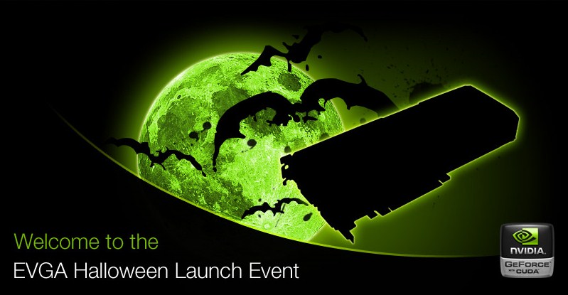
EVGA and NVIDIA are readying a unique multi-GPU graphics accelerator this Halloween, slated for October 30. To celebrate its launch, the two have organized a launch party for 300 lucky participants who will go to the NVIDIA Plaza in Santa Clara, CA and witness the launch of the new GeForce product. The accelerator packs two GPUs: a G200b, and a G92b. That's right, a GeForce GTX 200 series GPU, with a GeForce GTS 250 GPU. This is perhaps the first graphics accelerator to pack two entirely different GPUs. How it works, however, is interesting: the G200b GPU handles graphics, while the G92b is dedicated to PhysX processing. The accelerator could have 896 MB of graphics memory, with 512 MB of dedicated memory for the PhysX GPU.

EVGA and nVidia to launch a new Dual GPU card on Halloween
10/21/2009 by: Theo Valich - Get more from this author
Thanks to two members from SLIZone Forum, F34R and Obi-Wan Kenobi, we learned that nVidia is going to launch a new product on Halloweeen. Back on GPU Technology Conference, we were told that the company will launch a GeForce-based product "end of October" and "early November", but that seemed 2-3 weeks too early for Fermi, GT300/GF100-based desktop cards.
Thanks to two members from SLIZone Forum, F34R and Obi-Wan Kenobi, we learned that nVidia is going to launch a new product on Halloweeen. Back on GPU Technology Conference, we were toldEVGA and nVidia to launch a new Dual GPU card on Halloween
After checking out EVGA.com, we found a page in the news section that announces the event as well. As it turns out, EVGA and nVidia teamed up [or to be more precise - EVGA's engineering team delivered] and organized a launch party for 300 lucky participants who will come to nVidia's campus over at Santa Clara, CA and witness the launch of a new GeForce product. This kicked out interest into high gear, but being geographically dislocated [there are 'only' 6131 miles as the crow flies between my building and nVidia's Santa Clara campus] meant that we'll have to skip on the event. We turned to our sources and after few hours discovered the reason behind the event.
After talking to several people in the know, we managed to get to the bottom of this quite exciting announcement. While we don't have a final name for the card, it turns out that EVGA created a dual GPU card by combining GeForce GTS 250 with GeForce GTX 275. That's right, a dedicated PhysX GPU in the form of trusty G92 [debuted as 8800, rebranded as 9800, GTS 250 and GTX 260M/280M] and GT206/GT200b GPU for graphics. This is quite an interesting combination, to say the least. You're free to correct me in the comments if I am wrong - but I think this is the first time that any company took two different GPU chips and combined them on the same PCB. I've been a tech journalist for 10 years [Dec 15, 1999], but I never heard of such a combination.

As you can see in the crude mockup picture we created above [created with two images from colleagues at TechPowerUp!, image doesn't feature correct amount of memory chips], EVGA took the single PCB design from GeForce GTX 295, left one GeForce GTX 275 and simply placed a G92 GPU next to it. From one side, you have 896MB used by the GTX 275, and the second GPU - G92 uses only 512MB, making up for a never-seen-before 1408MB of GDDR3 video memory.
From our understanding, NVIO2 chip is connected to GTX 275, while GTS 250 cannot display an image at all. The sole purpose of GTS 250 is to be used for PhysX effects - during regular day in Windows, the G92b GPU sits in idle mode and consumers moderate amount of power. The chip is only powered up when PhysX gets into overdrive. Do note that the data mentioned above is our estimate.
We'll leave out a very interesting story about how come nVidia went into all that effort to create a single-PCB GTX 295 for another time, but the biggest thing about this announcement is EVGA. The company isn't afraid to wet its feet in non-reference board building, and after witnessing the launch of GTX 285 Classified, a triple 6-pin PEG connector graphics board for ultimate GPU overclocking [and a good exercise for upcoming Fermi-based GeForce 300 series] - we now have this quite interesting product.
We do not have information about the price, but we'll take an educated guess and estimate the price in the range between GeForce GTX 285 1GB and 2GB models [$349-419], going against the ATI Radeon HD 5850 and 5870. All in all, this is going to be quite an interesting Halloween. Can you say: "Trick or Treat?"

The answer: The card also calculates how a bat flies.